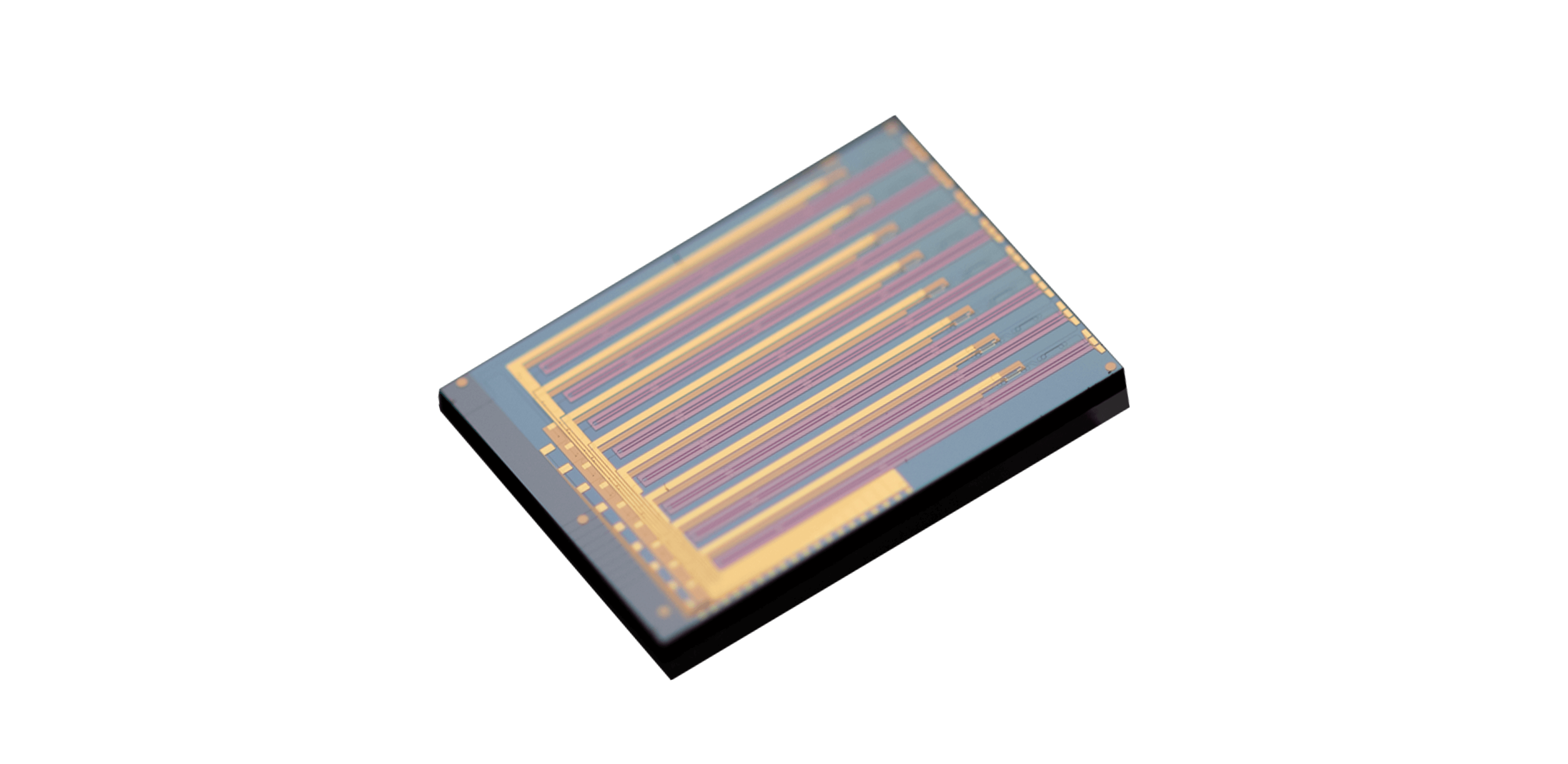
High-speed optical systems need devices that can control light quickly without demanding excessive voltage or consuming too much optical power. When they compare material platforms, thin-film lithium niobate is notable because it combines a strong electro-optic effect with compact, low-loss waveguides. That combination can expand the design options available to communication and measurement teams.
The opportunity is broader than one fast modulator. Integrated designs can combine active modulation with waveguides, splitters, resonators, filters, and polarization functions. They therefore examine the platform as a route to optical engines and subassemblies, while keeping packaging, electrical interfaces, thermal behavior, and production yield in the same technical conversation.
Current TFLN chips are increasingly discussed alongside photonic chips for data-center modules, coherent links, instruments, and sensing. They see their future value in the balance between bandwidth, drive efficiency, optical loss, and integration density, not in any one upper-end figure presented without system context.
Why Thin-Film Lithium Niobate Changes the Design Space
Thin-film processing places lithium niobate on a structure that supports tightly confined optical waveguides. This enables smaller bends and more complex circuits than traditional bulk devices, while retaining useful electro-optic properties.
They value the resulting design freedom because modulators and passive elements can be arranged for multi-channel architectures within a compact optical footprint. Liobate describes proprietary TFLN work that combines high electro-optic bandwidth, low drive voltage, and low insertion loss. For TFLN chips, these parameters influence lane rate, driver power, and link budget.
The benefit is clearer when fabrication and electrode design produce consistent results across channels and wafers rather than one optimized laboratory sample. Photonic chips built on this platform can support intensity modulation, IQ modulation, and polarization-division-multiplexed formats.
They assess which functions should be integrated and which should remain separate. Higher integration may reduce assembly count, but it can complicate yield, thermal control, test access, and replacement, so the product architecture must balance density with manufacturability.
Reading Chip Specifications Through a System Lens
Bandwidth specifications require careful interpretation. Liobate lists products from 70 GHz to 110 GHz, including a 3.2T DR8 chip at 110 GHz. They ask how the response was measured, which package or probe configuration was used, and how amplitude and phase behavior translate into the target waveform and error performance.
For TFLN chips, half-wave voltage affects driver requirements, while insertion loss determines how much laser power remains after modulation and coupling. Photonic chips must be evaluated through both parameters at once. A lower voltage may reduce electrical power, but the system benefit can be offset if optical loss or electrode loading requires compensation elsewhere.
Liobate specifies its 3.2T DR8 device with differential half-wave voltage below 1.5 V and insertion loss below 14 dB including coupling. They would place those numbers in a module model with laser output, splitter loss, receiver sensitivity, and thermal conditions. The aim is to confirm usable margin rather than repeat data-sheet figures without interpretation.
Moving from Early-Stage Devices to Repeatable Products
Moving from early-stage devices to repeatable products requires evidence that different circuit types can be fabricated, packaged, and tested consistently. Coherent applications provide a demanding example: Liobate lists a 1.6T or 800G ZR PDMIQ chip with 70 GHz bandwidth and insertion loss below 7 dB. They review channel balance, phase accuracy, bias control, polarization handling, and package interfaces because coherent performance depends on matched paths and stable complex modulation.
Photonic chips moving toward production need process design kits, documented design rules, wafer-level test, known-good-die strategy, and clear packaging references. TFLN chips also require repeatable fiber coupling and broadband electrical connections.
They consider these capabilities part of the product, since customers cannot build a scalable module from a die specification alone. Across bare dies, integrated chips, and related devices, they can evaluate what Liobate supplies. They would request statistical data, environmental results, sample traceability, and a clear distinction between typical values and committed specifications.
This helps module makers estimate yield and prevents a design from depending on performance that is not controlled in normal production. Design ownership should be clear across the supply chain.
Chip vendors, packaging houses, module makers, and equipment manufacturers need agreed interfaces and responsibility for failures. They establish data-sharing and change-review procedures early, because a performance shift at one process step may appear after final assembly and can otherwise be difficult to trace. Roadmaps should connect 800G, 1.6T, and 3.2T needs without assuming one chip fits every generation.
Different lane counts, reach classes, coherent or direct-detection formats, and package strategies may require separate designs. They value platform reuse where it reduces development effort, provided that each product retains sufficient optical and electrical margin.
Commercial adoption will depend on supply capacity, packaging partners, test throughput, change control, and technical support. A technically capable die has limited business value when customers cannot obtain consistent samples or transfer the design into volume assembly.
They therefore include manufacturing readiness in the same review as bandwidth and voltage. A useful TFLN roadmap connects the chip with packaging, test cost, and ownership across the supply chain. Statistical records from Liobate can help module developers decide whether the platform remains repeatable as builds move beyond engineering samples.
